Sony Semiconductor Solutions Corporation announced the upcoming release of the industry’s first stacked distance sensor IMX459 based on SPAD photon detectors for automotive LiDAR applications using direct time-of-flight (dToF).
The novelty combines tiny square pixels of single-photon avalanche diodes (SPADs) with a size of 10 microns and electronic circuitry for data processing and distance calculations on a single chip, resulting in a sensor in a compact form -factor with a standard size of 1 / 2.9, providing high accuracy and high speed of distance measurement.
The new sensor will contribute to the development of safe transport of the future by improving the detection and recognition characteristics in modern automotive LiDAR systems. This technology is essential for the massive adoption of Advanced Driver Assistance Systems (ADAS) and Autonomous Driving (AD) technologies.
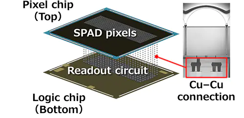
Among the various distance measurement methods in modern LiDAR systems, SPAD photon detectors are used as part of dToF sensors. They measure the distance to an object by determining the travel time (time difference) of light emitted from the source and returned to the sensor after being reflected from the object. Sony technologies such as backlit pixel structure, multilayer stacking configurations and Cu-Cu interconnects developed during the development of CMOS sensors, Sony has managed to obtain a device with a unique design that combines SPAD pixels and electronic distance computing in a single chip. … Thanks to this technology, the company was able to reduce the pixel size to ten microns, and thereby ensure a compact form of the device and achieve a high resolution, which is approximately 100 thousand effective pixels in a matrix format of 1 / 2.9. In addition, the new device features improved photon detection efficiency and improved sensitivity, providing high-speed, high-precision distance measurement with a resolution of up to 15 centimeters at both long and short ranges. The product complies with functional safety standards for vehicles, which helps to improve the reliability of LiDAR systems. At the same time, placing all this functionality on a single chip allows you to create even more compact and inexpensive LiDAR systems.
The product uses a stacking configuration in which a Cu-Cu connection provides contact between each pixel of the backlit SPAD (located at the top of the device) and the distance computing circuitry (at the bottom of the device). This approach makes it possible to obtain a structure in which the logic circuit is located under the pixels, while maintaining a high aperture ratio and a small pixel size – only 10 µm. In addition, the surface on which the light falls in the sensor has irregularities for its refraction, which makes it possible to increase the absorption rate. These features provide 24% high photon detection efficiency at 905 nm, which is widely used in laser light sources for automotive LiDAR systems. This makes it possible, for example, to detect distant objects with low reflectivity, with improved resolution and with a higher accuracy in determining the distance. In addition, the product features an active charging circuit available through the use of a Cu-Cu connection for each pixel, which normally provides a response time for each photon of approximately 6 nanoseconds.
This unique stacking configuration provides high speed and accuracy of distance measurement with a resolution within 15 cm both at long and short distances. This contributes to improved object detection and recognition performance in automotive LiDAR systems.
The product will pass AEC-Q100 Grade 2 certification for reliability testing of automotive electronic components. In addition, Sony has unveiled a development process that complies with ISO 26262 automotive functional safety standards and supports ASIL-B (D) functional safety requirements for failure detection, notification and control.
Prototype shipments are scheduled to begin March 2022 of the year.